BD96801Qxx-C
Configurable PMIC Including 4ch Switching DCDC Regulators and 3ch LDOs
BD96801Qxx-C
Configurable PMIC Including 4ch Switching DCDC Regulators and 3ch LDOs
BD96801Qxx-C is an automotive grade configurable PMIC (Power Management Integrated Circuit) with supporting Functional Safety features for application processors, SoCs and FPGAs. It has a scalable approach of output currents and rails by using internal MOSFET delivering up to 8A output or using external Driver MOS with 40A output.

主な仕様
機能安全:
特性:
ch
7
Vin1(Min.)[V]
2.7
Vin1(Max.)[V]
5.5
Output Voltage1 (Min.)[V]
0.5
Output Voltage1 (Max.)[V]
3.3
Output Current Capacity 1 [A]
2
Output Voltage2 (Min.)[V]
0.5
Output Voltage2 (Max.)[V]
3.3
Output Current Capacity 2 [A]
2
Output Voltage3 (Min.)[V]
0.5
Output Voltage3 (Max.)[V]
3.3
Output Current Capacity 3 [A]
4
Output Voltage4 (Min.)[V]
0.5
Output Voltage4 (Max.)[V]
3.3
Output Current Capacity 4 [A]
4
Output Voltage5 (Min.)[V]
0.3
Output Voltage5 (Max.)[V]
3.3
Output Current Capacity 5 [A]
0.3
Output Voltage6 (Min.)[V]
0.3
Output Voltage6 (Max.)[V]
3.3
Output Current Capacity 6 [A]
0.3
Output Voltage7 (Min.)[V]
0.3
Output Voltage7 (Max.)[V]
3.3
Output Current Capacity 7 [A]
0.3
SW frequency(Max.)[MHz]
2.25
Circuit Current(Typ.)[mA]
8.2
Shutdown Current (Typ.)[uA]
0
Serial I/F
I2C
Operating Temperature (Min.)[°C]
-40
Operating Temperature (Max.)[°C]
125
Package Size [mm]
6.0x6.0 (t=1.0)
Common Standard
AEC-Q100 (Automotive Grade)
特長:
- AEC-Q100 Qualified. (Grade 1)
- ISO 26262 Process Compliant to Support ASIL-D.
- Ultra-high Buck Switching Frequency up to 4MHz.
- Built-in MOSFETs or External Driver MOS.
(BD96340MFF-C) Selectable for BUCK1 and BUCK2. - Built-in MOSFETs for BUCK3 and BUCK4.
- Dual Phase Operation for BUCK1 and BUCK2.
- Dual Phase Operation for BUCK3 and BUCK4.
- Remote Sensing for Accurate Voltage at the Point of Load.
- Multipurpose LDO for LDO5, 6.
- Load Switch or LDO Selectable for LDO7 Output.
- Programmable Power Squencer by OTP (One-time Programmable memory), EEPROM, or I²C.
- High Precision Built-in Supervision.
OVD (Over Voltage Detection), UVD (Under Voltage Detection) , TW (Thermal Warning). - Built-in Protection.
OVP (Over Voltage Protection), UVP (Under Voltage Protection), TSD (Thermal Shutdown) - Built-in UVLO (Under Voltage Lockout) for VIN, PVIN1 to PVIN7, and VREG15IN.
- Built-in Digital Self-test for OTP, Power Sequence, and Detection.
- Built-in Analog Self-test for Detection.
- Built-in Self-test for Critical Signal Pins (PRSTB, INTB_ADDPRSTB1, EN).
- Built-in Mutual Monitoring of VREF and OSC.
- Q&A Watchdog Timer.
- I²C Support Fast Mode (Max 400kHz) and Fast Mode Plus (Max 1MHz) with CRC.
リファレンスデザイン / アプリケーション評価キット
-
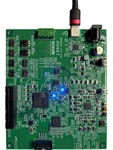
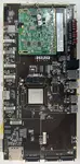
- Evaluation Board - BD96801-EVK-302
The evaluation board has been designed to be used as a daughter board(DB) in combination with the main board PMIC-MB-EVK(MB) and the software GUI interface. It can also be operated in stand-alone mode without GUI software. The BD96801 contains 4 buck converters and 3 LDOs that can be flexibly configured via factory OTP settings, user EEPROM settings or I2C commands.
-
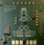
- Reference Design - REF67001
- AMD FPGA Spartan7/Artix7プラットフォーム向けリファレンスデザイン
本リファレンスデザインはAvnet様と協同で作成した産機向けに使用されるAMDのSpartan7/Artix7向けの電源リファレンスボードです。FPGAに電源供給するPMICにはOTP (One Time Programmable Memory) 機能を搭載し出力電圧・シーケンスの設定ができるScalable PMIC BD96801Qxx-C を活用し、あらかじめSpartan7/Artix7に必要な電源電圧・シーケンスをOTPにて設定したArtix7/Spartan7専用PMIC BD96801Q30-Cを搭載しております。
-
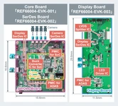
- Reference Design - REF66004
- SemiDrive 次世代コクピットSoC 「X9M/X9E」 電源/インターフェースソリューション
ロームは、SemiDrive社の次世代コクピットSoC「X9M/X9E」に最適な電源/インターフェースのリファレンスデザインを開発しました。「X9M/X9E」に最適な電源/インターフェースのリファレンスデザインを提供することにより、設計者の開発負荷の軽減と市場の要求する性能の達成に貢献します。今回リファレンスデザインを開発したSemiDriveの最新の車載SoC「X9M/X9E」は、コクピットをはじめ、さまざまな車載アプリケーションの高機能化に貢献します。
SemiDrive社の次世代コクピットSoC「X9M/X9E」についての問い合わせはこちら

- 「X9M/X9E」の使用に最適化されたScalable PMIC(BD96801Q12)
- 車載カメラモジュールに最適なSerDes IC(BU18xMxx)
- マルチ画面化する車載ディスプレイに向け、フルHD(1,980×1,080ピクセル)対応のSerDes IC(BU18xL82)
- 車載ディスプレイの機能安全に貢献するInterface IC(BU92RTF82)
- 車載向け2.7V~5.5V入力 12A MOSFET内蔵 1ch降圧DC-DCコンバータ (BD9SA01F80)
本リファレンスデザインは3枚の基板で構成されています。
- REF66004-EVK-001 (Core Board)
- REF66004-EVK-002 (SerDes Board)
- REF66004-EVK-003 (Display Board)
関連ニュース:
-
- Reference Design - REF66012
- ADAS SoC用 PMICソリューション リファレンスデザイン
インテリジェントフロントカメラ (IFC) は200万ピクセルの高解像度カメラを統合し、L2レベルの前方ADAS機能を実装できる複数のミリ波レーダーへのアクセスをサポートします。このソリューションは、4TOPS AIコンピューティング能力を備えたHorizon Journey2チップとInfineon TRAVEO IIシリーズCYT4BFマイクロコントローラーを使用します。Horizon Journey2に対応する視覚アルゴリズムを導入して障害物、車線、その他の交通要素を識別し、車両センサーフュージョンと車両制御にInfineon TRAVEO II シリーズCYT4BFマイクロコントローラーを使用することにより、このソリューションはAEB、ACC、LCC、そしてTJAなどのADAS機能を実現できます。BD96801Q09やBD9S303MUFなど、ASIL D機能安全レベルのロームPMICチップを選択することで、インテリジェントフロントカメラ(IFC)の信頼性と安定性を確保できます。
Intron Technology社とのコラボレーションボード
Intron Technologyは、中国で急成長している自動車エレクトロニクス・ソリューション・プロバイダーです。新エネルギー、車体制御、安全、パワートレイン・システムなどに応用される重要な自動車用電子部品をターゲットとしたソリューションの提供に注力しています。研究開発およびエンジニアリング能力を活用し、先進的な半導体デバイスを組み込んだソリューションを提供することで、OEMが業界をリードする性能を達成できるよう支援しています。

-
- Reference Design - REF67003
- Telechips インフォテインメント及びコックピットSoC「Dolphin3」 電源ソリューション
ロームは、Telechips社のコクピットSoC「Dolphin3」に最適な電源ソリューションのリファレンスデザインを開発しました。「Dolphin3」に最適な電源のリファレンスデザインを提供することにより、設計者の開発負荷の軽減と市場の要求する性能の達成に貢献します。今回リファレンスデザインを開発したTelechips社の車載SoC「Dolphin3」は、コクピットをはじめ、さまざまな車載アプリケーションの高機能化に貢献します。
Telechips社のコクピットSoC「Dolphin3」についての問い合わせは こちら
「Dolphin3」の使用に最適化されたConfigurable PMIC(BD96801Qxx-C)
関連ニュース:
2024年11月21日 - ロームのSoC向けPMICが、総合半導体ファブレスメーカーTelechipsの次世代コックピット向け電源リファレンスデザインに採用
